


Global unterwegs / im Detail zu Hause
Die PVA TePla AG ist ein weltweit agierender Verbund vielseitiger Hochtechnologieunternehmen. Mit jahrzehntelanger Erfahrung und dem Blick für die Innovationen von morgen entwickeln wir konkurrenzlose Anlagen für Vakuum-, Hochtemperatur- und Plasmaprozesse sowie für die Qualitätsinspektion - immer in enger Zusammenarbeit mit unseren Kunden.
PVA TePla / Beteiligungen
Vacuum & Nitriding Systems
Die Industrial Vacuum Systems ist Marktführer für Druck-Sinteranlagen, Hochvakuum-Lötöfen und Diffussionsschweißanlagen für großformatige Bauteile — etablierter Lieferant für induktiv beheizte Vakuum-Schmelz-, Gieß- sowie Plasma-Nitrieranlagen.

Metrology & Plasma Solutions
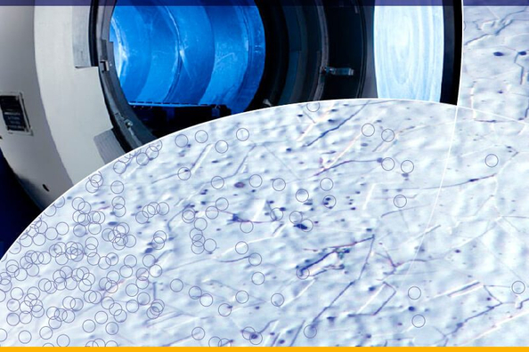
Plasma Anlagen und IR-Messsysteme zur Reinigung und Entfernung von organischen Schichten sowie zur Qualitätsinspektion und Überwachung von Fertigungsprozessen in der modernen Halbleiterindustrie, beispielsweise von Scherstress in Wafern, zur Implantationskontrolle und Oberflächeninspektion.
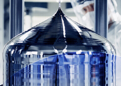
Crystal Growing Systems
Seit 60 Jahren ist die Crystal Growing Systems führender Systemlieferant von Kristallzuchtanlagen für die Halbleiter- und Photovoltaikindustrie — Floating-Zone- und Czochralski-Systeme für ultrareine Silizium- und Germanium-Kristalle.

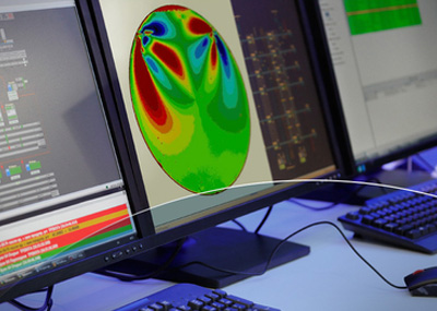
Scanning Acoustic Microscopy
Die Analytical Systems entwickelt Anlagen zur Ultraschall-Inspektion, insbesondere für Kristallzuchtanlagen und optische Analysesysteme für die Halbleiterindustrie. Alleinstellungsmerkmale sind die besonders feine Auflösung und die Inspektion von 300mm-Silizium-Ingots.

Vacuum Processing Service
Mehr als 15 Jahre steht die Löt- und Werkstofftechnik im Zeichen individueller Vakuumprozesstechnik zum Vakuumlöten, Diffusionsschweißen und zur Vakuumwärmebehandlung — komplettiert durch eine fügetechnische Bauteil- und Materialberatung.
Software Production Automation
Die SPA Software Entwicklungs GmbH bedient Kunden weltweit mit spezifischen Softwareprogrammen für die industrielle Automatisierung von Produktionssystemen. Stark im Bereich der Halbleiterindustrie bietet sie komplette Systeme mit hochpräziser Messtechnik sowie die Bilderfassung mit dazugehöriger Datenanalyse zur Waferinspektion an.