


PVA TePla is an association of diverse high-tech companies that operate worldwide. Backed by decades of experience and an eye for the innovations of tomorrow, we develop unrivaled systems for vacuum, high-temperature, and plasma processes as well as for quality inspections—always in close cooperation with our customers.
Vacuum & Nitriding Systems
Industrial Vacuum Sytems is a market leader for pressure sintering systems, high-vacuum brazing furnaces, and diffusion bonding systems for large components—an established supplier of inductively heated vacuum melting and casting systems as well as plasma nitriding systems.


Metrology & Plasma Solutions
Plasma systems and IR measuring systems for cleaning and removing organic layers and for quality inspection and monitoring production processes in the modern semiconductor industry, for example, shearing stress in wafers, for implant process monitoring, and surface inspection.
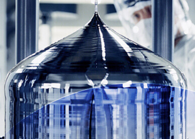
Crystal Growing Systems
For over 60 years, Crystal Growing Systems is a leading supplier of crystal growing systems for the semiconductor and photovoltaic industry—floating zone and Czochralski systems for ultra-pure silicon and germanium crystals.

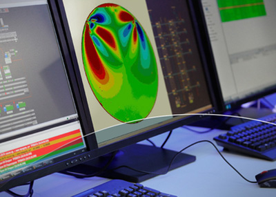
Scanning Acoustic Microscopy
Analytical Systems offers system development for ultrasound inspection systems, especially for crystal growing systems and optical analysis systems for the semiconductor industry. Unique features include the exceptionally high resolution and the ability to inspect 300 mm silicon ingots.


Vacuum Processing Service
Loet- und Werkstofftechnik is leading the way for over 15 years In the field of vacuum process technologies for vacuum brazing, diffusion bonding, and vacuum heat treatment—rounded out with component and material advice with regard to joining technology.
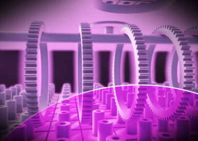
Software Production Automation
SPA Software Entwicklungs GmbH serves customers worldwide with specific software programs for the industrial automation of production systems.
Strong in the semiconductor industry they offer complete systems with high-precision measurement technology as well as image acquisition with associated data analysis for wafer inspection.