
Pinmarks can be revealed on the basis of characteristic stress fields. The automatic detection and quantification of pinmarks caused by process tools is one of the most important tasks while monitoring the quality of temperature treated wafers in a production environment.
Fig.1: Color scale SIRD differential depolarization image of a 300mm-Epiwafer
Figure 1 shows a high temperature processed wafer after treatment in a RTP chamber. The chamber tools (wafer support pins) leave their own finger print in form of so called pinmarks (red marked).
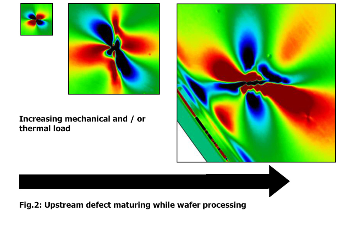
The shear stress field of such a pinmark (zoom) reminds to a flower or a butterfly.
Pinmarks show typically different stages of evolution during the production. At the very beginning of the wafer stadium, the tool supporting pin presses a small plug into the wafer during a high temperature process. At this state we can observe the typical symmetric wings.
After several process steps, these features start to get more and more structured. A degradation of shape and symmetry can be monitored (Fig.2).
Fig.2: Upstream defect maturing while wafer processing Figure 2 shows one defect after different processing steps. At the beginning we can observe a symmetric feature, in the middle there is an internal structure and at the last state we can observe a risky slip line. To detect and quantify such pinmarks we have developed the real image processing tool “SIRD Vision” for automated pinmark detection. The first step of this intelligent tool is to find pinmaks and pinmark related defects on the wafer and to mark and label them.
Fig.3: Pinmark defects automated recognized and labeled by SIRD Vision software
Figure 3 shows the SIRD Vision automated foundings of pinmarks and marking these. SIRD Vision works likely as a face detector in a modern smart phone. After successful pinmark detection, the novel software analyses these findings. On the basis of direct measurement data, the pinmarks are investigated for its properties.
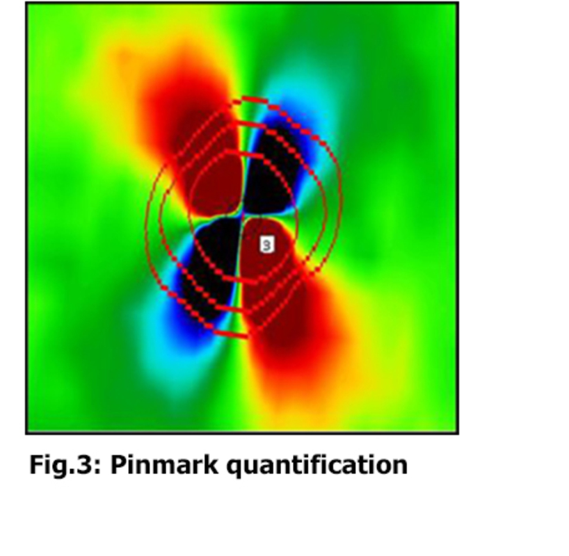
Fig.3: Pinmark quantification
Figure 3 shows the pinmark quantification process. Different and specialized mathematical functions scan these defects for different properties at different positions (indicated by red lines).
The output of such a pinmark investigation is a (Excel)table with several indication values.
The most important values are:
- Class of pinmark (number of coherent wings)
- Complexity (symmetry deviation of shape)
- Decay (decline factor)
- Strength (the direct force)
The analysis values for this example would be :
| Class | Complexity | Decay | Strength[Pa] |
| 2 | 4.3 | 1.7 | 19.73k |
Tab.1: Pinmark quantification results
Table1 lists the most important investigation values of the example.
The whole automated combination of measurement, image processing and defect analysis makes the SIRD to a powerful tool.
Process and reactor control can be done easily by comparable and automated values, generated direct after the wafer measurement.
Consequently SIRD and SIRD Vision are on the cutting-edge of technology for save wafer handling and production.
Author: Dr. M. Wagner, G. Kupka ; PVA TePla MPS laser division