- PVA TePla
- Technology Fields
- Quality Inspection
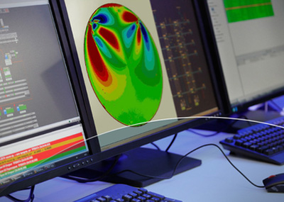
Our SIRD systems enable
- Reliable monitoring of epitaxy reactors with a particular focus on the wafer edge region
- Monitoring and optimizing of high-temperature or abrasive processes in the manufacturing of silicon wafers for semiconductor components, solar cells, and other materials for opto-electronic components
- The evaluation of global stress or localized defects both on the entire silicon wafer as well as in defined areas
Learn More about the Technology
Metrology & Plasma Solutions
With our VPD method (Vapor Phase Decomposition), we enable
- Reliable analysis of wafers and semiconductor components to a concentration range of 107 at/cm²
- Etching of the wafer surface with gaseous hydrogen fluoride (HF) to ensure absolute purity and safe handling of the HF gases.
- Collection of contamination and concentration in a small droplet using the PAD scan. This module offers various scan patterns, advanced handling of droplets, and preparation of the subsequent analysis.
- Preparation for the Analysis
Learn More about the Technology
Metrology & Plasma Solutions
Our SAM systems and software provide options for
- Non-destructive testing of opaque (optically non-transparent) materials for quality and process control as well as for research applications
- Fully-automated detection of cavities, voids, bubbles, inclusions, and delamination—particularly suitable for wafer inspection, bond checking, and MEMS inspection.
- Combinations of ultrasonic microscopy and optical microscopy—particularly suitable for research and industrial applications
- Analysis and evaluation of specific customer samples
Learn More about the Technology
Scanning Acoustic Microscopy